TPS61291 features: 0.9V to 5V input voltage range; 7.5μA quiescent current in boost mode; internal feedback divider disconnected (bypass mode); overtemperature protection
Typical application range of TPS61291: measurement (gas meter, water meter, smart meter); remote control device; residential security / home automation
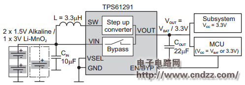
TPS61291 reference design application circuit:

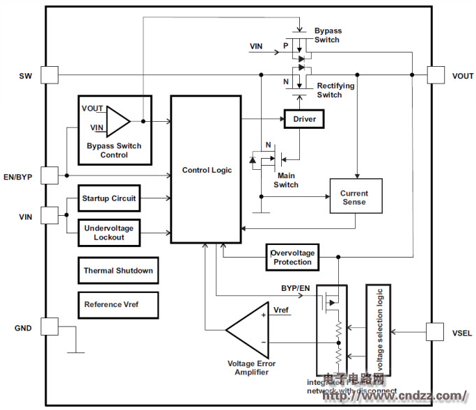
Figure 1 TPS61291 internal structure diagram
The TPS61291 provides two operating modes: high efficiency boost mode to generate an output voltage higher than the input voltage and bypass mode, which connects the output of the device directly to the input.

Figure 2 TPS61291 reference design
The TPS61291 is a boost converter with pin selectable output voltages and an integrated bypass mode. In bypass operation, the device provides a direct path from the input to the system and allows a low power microcontroller (MCU) to operate directly from a single 3V Li -MnO2 battery or dual alkaline battery cells.
TPS61291 Chinese data sheet: Click to download
More schematics and source code popular application circuit: click now
Wuxi Motian Signage Co., Ltd , https://www.makesignage.com