Andy Jolly is a senior application consultant – the program is Synopsys' global product line leader, FPGA-based prototyping. Andy has been engaged in FPGA technology research and development for more than 25 years. Recently, he has begun to provide support to customers to support their complex CPU SoC and GPU IP prototyping needs on the Synopsys HAPS platform, while supporting the development of the same SoC and GPU IP embedded in user programs worldwide. .

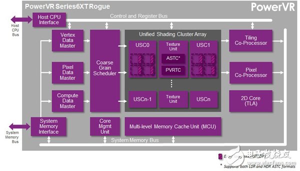
The PowerVR Rogue GPU is built on the principle of efficiency and market leadership, which has significantly improved the performance of past generations of image processors. To achieve high performance, the GPU architecture leverages powerful parallel processing power to handle demanding image and computing tasks. When configuring GPU IP for high performance, the design team is faced with multiple challenges. They need to incorporate complex, high-gate designs into the limited space of a single FPGA. Considering the scalability of the Series 6, Series 6XE, and Series 6XT families (from half to eight clusters), there are more challenges when trying to test these complex devices.

The PowerVR Series6XT GPU scales from two clusters to eight clusters. As the process of other options (ie, manufacturing test chips) became more expensive and time consuming, Synopsys and Imagina TIon worked together to create a more dynamic FPGA-based prototyping architecture. As a result, new optimization processes using multiple FPGAs and even the largest PowerVR GPU modeling are available. The following will specifically show the experience of obtaining this achievement.
GPU prototyping requirements
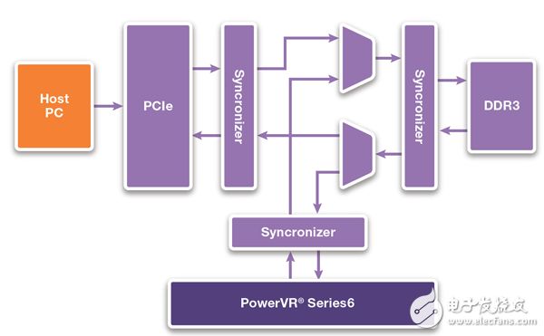
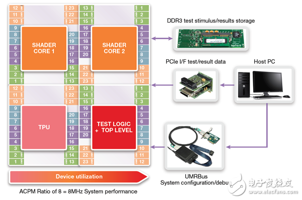
The first step Synopsys did was to launch a proof of concept project. This project demonstrates an FPGA-based prototyping for ImaginaTIon's PowerVR Series6 GPU. The prototyping environment includes a top-level test architecture for independent regression testing. The test architecture connects to the host PC via the PCIe port and the storage test stimulus and results using the DDR3 storage interface. This allows the test team to control and analyze the GPU and configure the system via the Universal MulTI-Resource BUS (UMRBus) and access test and result data from the host PC.

Top-level test architecture supporting regression testing
The team manually designed the implementation of the Synopsys HAPS-70 S48 prototyping system with multiple FPGAs, achieving clock speeds of several MHz. 7000 regression tests will be implemented on the system - all tests do not require a test chip. We not only differentiate derivative designs (even larger devices than Series6 GPUs), but also create additional test logic and sufficient performance to support video output. This can be done by using ProtoCompiler. ProtoCompiler is Synopsys' second-generation FPGA automation differentiation tool. ProtoCompiler is designed to minimize the time and effort required for startup, and then deploy the Synopsys HAPS family of systems for IP verification and software development. It combines automation features for design planning, logic synthesis, debugging, and connectivity to other verification environments such as Synopsys VCS and ZeBu. Prototyping software is tightly integrated with the HAPS series to provide system performance.
The success of the PowerVR Series6 and Series6XT prototypes means that the ImaginaTIon design team seldom relies on the use of test chips when bringing new GPUs to market. Early access to the prototype ensures system verification, early software development, and simplified software and hardware integration.

PowerVR Series6 GPU in Synopsys HAPS-70
The ultimate 12 MHz performance with the prototyping platform enabled Imagination to perform thousands of tests in a matter of hours and provide early software development for the platform. In addition, the HAPS system supports video output to allow real-time, working I/O to check the correctness and quality of image processing.
Plug-in Type Cassette PLC Splitter
PLC Planar Waveguide Optical Splitter (PLC Splitter) is an integrated waveguide optical power distribution device based on a quartz substrate. Like coaxial cable transmission systems, optical network systems also need to couple, branch, and distribute optical signals. Need Optical Splitter to realize.
Plc Splitter is one of the most important passive components in optical fiber links. It is an optical fiber tandem device with multiple input ends and multiple output ends. It is especially suitable for connecting the central office and the central office in passive optical networks (EPON, GPON, BPON, etc.) Terminal equipment and realize the branch of the optical signal.
The advantages for PLC Splitter:
(1) Loss is not sensitive to the wavelength of the transmitted light, and can meet the transmission needs of different wavelengths.
(2) The light is evenly split, and the signal can be evenly distributed to users.
(3) The structure is compact and the volume is small, and it can be directly installed in various existing transfer boxes without special design to leave a lot of installation space.
(4) There are many shunt channels for a single device, which can reach more than 32 channels.
(5) The multi-channel cost is low, and the more the number of branches, the more obvious the cost advantage.
Cassette Plc Splitter,Plug-In Plc,Plug-In Type Cassette Plc Splitter,Optic Fiber Splitter
Shenzhen GL-COM Technology CO.,LTD. , https://www.szglcom.com