In traditional FPGA design, oscilloscopes and logic analyzers are mostly used for debugging. FPGA and PCB designers reserve a certain number of FPGA pins as test pins. When the FPGA designer writes the FPGA code, the FPGA internal signals that need to be observed are defined as the output of the module, and these signals are locked to the reserved state during the integrated implementation. On the test pins, the probes of the oscilloscope or logic analyzer are connected to these test pins for observation. This test method has many limitations, high cost, poor flexibility, and troublesome operation.
high cost. The cost of an oscilloscope and logic analyzer is high.
Poor flexibility. To test the internal nodes of the FPGA, you need to modify the design and bring the signal to be tested to the FPGA pin for testing. After the PCB design is completed, the number and number of these pins used as test pins are fixed and cannot be changed flexibly. If the test pin is not enough, it will affect the test. If there are too many test pins, it will affect the PCB layout and wiring. And in some extreme designs, the I/O pins of the FPGA may have been used up, and no extra pins are used to test pins.
The operation is troublesome. The oscilloscope and logic analyzer must be connected to the test pins through the probe, which can easily cause a short circuit and damage the device.
As the scale of FPGAs continues to increase, the design of FPGAs becomes more and more complex, and the package form is mostly shifted to a spherical mode. The traditional way of using probes to monitor signals becomes more and more difficult. Xilinx's integrated logic analysis tool, ChipScope Pro, completely solves these problems.
ChipScope Pro has the features of a traditional logic analyzer, is inexpensive, and does not require a large number of probes, which is highly practical. It is an on-chip logic analysis tool designed for the Xilinx Virtex series and Spartan series devices. It uses the JTAG port to read out the internal signals of the FPGA and send them to the computer for analysis. The basic method is to use the BRAM in the FPGA to store the signal waveform data, then transfer the data to the computer through the JTAG interface and display the waveform on the computer. Figure 9-1 shows the connection structure of the ChipScope test system.
The use of this technique to observe the test method of the internal signal of the FPGA has the following advantages.
The cost is lower. Only ChipScope Pro design software and a download cable are required, which greatly simplifies PCB design costs.
Higher flexibility. It is not necessary to output the signal to be observed to the FPGA through an extra pin. The number of signals and the depth of storage are determined by the device BRAM. The more BRAM in the device, the greater the number of observable signals and the depth of storage.
Easy to use. ChipScope Pro is called as an IP module in the ISE tool, which allows you to easily select the signal to be tested or set up complex trigger conditions.
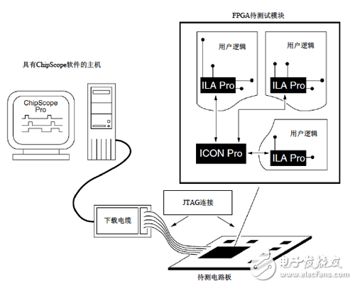
Figure 9-1 ChipScope test system connection structure
ChipScope Pro consists of a series of related IP cores and their software tools, including Core Generator, Core Inserter, ChipScope Analyzer and TCL Script Control Interface.
(1) Nuclear generator
Xilinx Core Generator Tool: It can generate netlists for Integrated Controller Core (ICON), Integrated Logic Analysis Core (ILA), Virtual I/O Core (VIO), and Agilent Tracking Core (ATC2). Instantiate the required template files.
IBERT Core Generator: Generates the netlists for the Virtex-4 and Virtex-5 series of bit error rate test cores (IBERT) and the template files needed for instantiation.
(2) Nuclear inserter
Core Inserter: Automatically inserts the CON, ILA, and ATC2 cores into a design that has been integrated.
PlanAhead Design Analysis Tool: Automatically inserts ICON and ILA cores into the design netlist. Please refer to the PlanAhead chapter.
(3) ChipScope Analyzer (ChipScope Analysis Software): It can configure the FPGA, set the trigger condition, and set the trace display mode of ILA, IBA/OPB, IBA/PLB, VIO and IBERT.
(4) ChipScope Engine Tcl (CSE/Tcl) ScripTIng Interface: The communication interaction with the chip is completed through the TCL scripting language and the JTAG chain. In the design, there are two operational procedures for using ChipScope Pro, as shown in Figure 9-2.
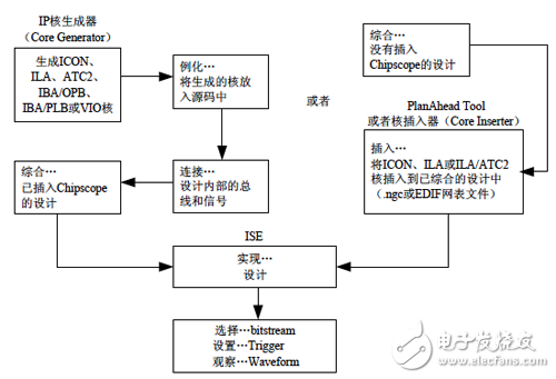
Figure 9-2 ChipScope operation flow chart
Process 1: Through the ChipScope Pro kernel generator, various debugging functions such as ICON, ILA, and IBA are generated, and the generated instantiation code is inserted into the HDL source program, and then the design including the ChipScope Pro core is integrated. Download to the device and analyze with the ChipScope Analyzer.
Process 2: Use ChipScope Pro's kernel inserter to insert the required kernel directly into the already completed design netlist (NGC or EDIF), then route the new netlist file and download it to the device, using ChipScope. Analyzer for analysis.
Next, we will introduce ChipScope's IP core and its application in detail, focusing on the following.
ChipScope Pro core generator and the properties of each core.
ChipScope kernel inserter.
ChipScope Pro Analyzer nuclear analyzer.
Modify the ChipScope core signal connection in the FPGA Editor.

Whaylan 600W portale power stations have Large capacity, high endurance, a variety of ports, at any time for your need to charge the equipment. Completely say goodbye to the anxiety of outdoor electricity and devote yourself to an outdoor activity. At the same time, it can be equipped with solar panels to charge the power supply. The energy storage technology of lithium battery is combined with the clean renewable energy of solar energy to truly realize the enjoyment from day to night.
600W power station,solar station,bluetti 600w,lithium generator
suzhou whaylan new energy technology co., ltd , https://www.whaylan.com