The switch acts as a turn-on or turn-off signal in the circuit. The most common controllable switch is a relay. When a high or low level is applied to the drive circuit of the drive relay, the relay is pulled or released, and its contacts are turned on or off. The CMOS analog switch is a controllable switch. It can be used in high current and high voltage applications unlike relays. It is only suitable for processing analog or digital signals whose amplitude does not exceed its operating voltage and current.
First, commonly used CMOS analog switch pin function and working principle 1. Four bidirectional analog switch CD4066
The pin function of the CD4066 is shown in Figure 1. There are 4 independent analog switches inside each package. Each analog switch has three terminals: input, output and control. The input and output are interchangeable. When the control terminal is high, the switch is turned on; when the control terminal is low, the switch is turned off. When the analog switch is turned on, the on-resistance is several tens of ohms; when the analog switch is turned off, it exhibits a high impedance and can be regarded as an open circuit. The analog switch can transmit digital signals and analog signals. The upper limit of the transmittable analog signal is 40MHz. The crosstalk between the switches is small, typically -50dB. 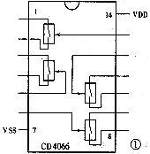
Figure 1 Pin function of CD4066 2. Single eight-way analog switch CD4051
The CD4051 pin function is shown in Figure 2. The CD4051 is equivalent to a single-pole, eight-throw switch. Which channel the switch is connected to is determined by the input 3-bit address code ABC. The truth table is shown in Table 1. “INH†is the prohibited end. When “INHâ€=1, each channel is not connected. In addition, the CD4051 is equipped with another power supply terminal VEE for use as a level shift, so that the digital signal provided by the CMOS circuit normally operating under a single power supply can directly control the multiplex switch and This multiplexer transmits AC signals with peak-to-peak values ​​up to 15V. For example, if the power supply of the analog switch is VDD=+5V, VSS=0V, when VEE=-5V, as long as the digital control signal of 0~5V is applied to the analog switch, the analog signal with amplitude range of -5V to +5V can be controlled. . 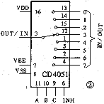
Figure 2 CD4051 pin function table 1 CD4051 truth table 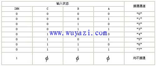
3. Double four-way analog switch CD4052
The pin function of the CD4052 is shown in Figure 3. The CD4052 is equivalent to a double-pole, four-throw switch. Which channel is specifically connected is determined by the input address code AB. The truth table is shown in Table 2. 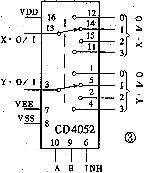
Figure 3 Pin function of CD4052 Table 2 CD4052 truth table 
4. Three sets of two-way analog switch CD4053
The pin function of the CD4053 is shown in Figure 4. The CD4053 contains three sets of single-pole double-throw switches. Which one of the three sets of switches is connected is determined by the input address code ABC. The truth table is shown in Table 3. 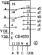
Figure 4 Pin function of CD4053 Table 3 CD4053 truth table 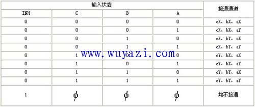
5. Sixteen analog switch CD4067
The pin function of the CD4067 is shown in Figure 5. The CD4067 is equivalent to a single-pole, six-throw switch. Which channel is specifically connected is determined by the input address code ABCD. The truth table is shown in Table 4. 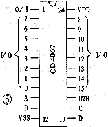
Figure 5 Pin function of CD4067 Table 4 CD4067 truth table 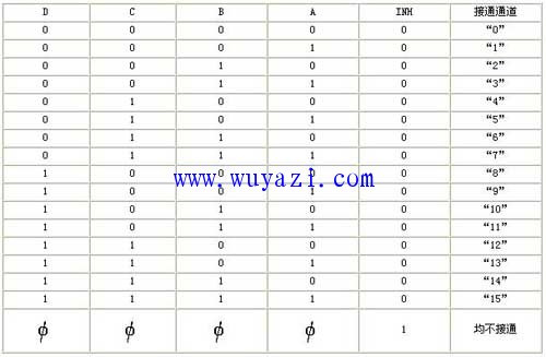
Second, the typical application example 1. Single button volume controller single button volume controller circuit shown in Figure 6. The VMOS tube VT1 is connected as a variable resistor between the output of the volume potentiometer of the audio device and the ground. The resistance between the D and S poles of VT1 varies inversely with VGS, so controlling the VGS allows control of the volume. The G pole of VT1 is connected to three analog switches S1 to S3 and a 100μF capacitor, wherein the 100μF capacitor acts as a voltage hold. Since the resistance between the G and S poles of the VMOS tube is extremely high, the voltage on the 100 μF capacitor can remain substantially constant for a long time. The analog switch S1 provides a charging circuit for the capacitor. When S1 is turned on, the power supply charges the capacitor through S1, and the voltage on the capacitor is continuously increased, so that the on-resistance of the VT1 is getting smaller and smaller, and the volume is getting smaller and smaller. The analog switch S2 provides a discharge loop for the capacitor. When S2 is turned on, the capacitor is discharged through S2, and the voltage on the capacitor is continuously decreased, so that the volume is getting larger and larger. The analog switch S3 is activated by the power-on volume. When the power is turned on, the power supply generates a short positive pulse at the S3 control terminal, so that the S3 is turned on. Since the resistance connected to the S3 is small, the capacitor is quickly charged to a certain voltage, so that the capacitor is quickly charged to a certain voltage. The starting volume is in a small state. F1 ~ F6 and its peripheral components constitute a long and short pulse identification circuit. When static, the F1 and F2 inputs are high. When the button switch AN is pressed for a long time, the F4 output goes high, and the 3.3μF capacitor is charged through the 100k resistor. When the charging voltage exceeds the CMOS gate switching voltage, the F5 output is high. It goes low, the output of F6 changes from low to high, the analog switch S2 is turned on, the 100μF capacitor is discharged, and the volume becomes louder. At the same time, the F1 output also becomes high, and the capacitor is also charged, but the positive jump of the F1 output is not enough to make the voltage on the capacitor exceed the conversion voltage, so the F2 output is still high, F3 outputs low level, analog switch S1 remains cut off. When the button switch AN is continuously pressed, the F4 output also changes continuously. When the output is high, the capacitor is charged, and when the output goes low, the capacitor is quickly discharged through the diode VD3, so the voltage on the capacitor always fails to reach the conversion voltage. Therefore, the F6 output is always low. At this time, the F1 output continuously changes in high and low frequency, and the capacitor is charged by the diode rectification, so that the voltage on the 3.3μF capacitor quickly reaches the conversion voltage, the F2 output becomes low, the F3 output becomes high, the analog switch S1 is turned on, the capacitor is charged, and the volume is changed. small. Thus, the size control of the volume is achieved by using a push button switch. 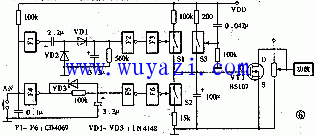
Figure 6 Single button volume controller circuit 2. Four-channel video signal switcher The four-channel video signal switch circuit is shown in Figure 7. The NAND gates YF3 and YF4 form a pulse oscillator, and the oscillation frequency is adjusted by a 100k potentiometer. If the adjustment range is not enough, the 0.47μF capacitor and 100k resistor can be replaced appropriately. The pulse oscillator is controlled by the bistable circuit composed of YF1 and YF2. When S1 is pressed, YF1 outputs a low level, and the pulse oscillator stops. When S2 is pressed, YF1 outputs a high level, and the pulse oscillator starts to oscillate. The output of the pulse oscillator is used as the clock of the CD4017 decimal counter, so that Y0~Y3 sequentially appear high level, and the corresponding four analog switches are turned on in turn, and the video signals input by Vi1~Vi4 are sequentially switched to the output end, and four are completed. Switching of the video signal of the road. Obviously, adding a CD4066 can be made into an eight-way video signal switcher. Accordingly, analog switch control is performed from Y0 to Y7, and Y8 is connected to Cr. And so on, can make more channels of video signal switcher. Moreover, the input and output can also be other forms of signals. If the video and audio signals are required to be transmitted simultaneously, the corresponding number of analog switches can be connected. 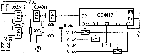
Figure 7 four-way video signal switcher circuit
Explosion Proof Motor,Explosion Proof Servo Motor,Exproof Motors,Explosion Proof Ac Motor
Yizheng Beide Material Co., Ltd. , https://www.beidevendor.com