The signal source is one of the four general electronic measuring instruments, the other three are: network analyzers, spectrum analyzers and oscilloscopes. This introduces the basics involved in signal sources. The most common function of the source is to generate a sine wave, so start with the introduction of the characteristics of the sine wave.
First, the signal characteristics of the sine waveThrough the expression equation of the sine wave signal, the parameters contained in the signal can be reflected as: signal amplitude; frequency; initial phase. The frequency and initial phase of the signal can be included in the phase information of the signal.
For an ideal sine wave signal, its amplitude and frequency and initial phase should be deterministic parameters, so the sine wave signal is a relatively simple signal. Defining a continuous wave signal requires only two aspects of amplitude and frequency.
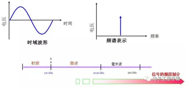
Figure 1 Sine wave signal characteristics
Typical amplitude parameters for a sine wave generated by a signal source are as follows:
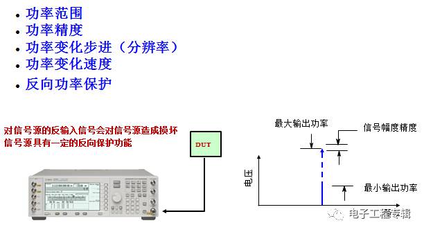
Figure 2 Typical amplitude parameters of the sine wave output from the signal source
Signal sources should consider amplitude accuracy to improve test repeatability and reduce test uncertainty.
The typical frequency parameters of the signal source are as follows:
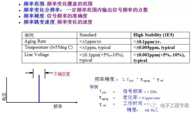
Figure 3 Typical frequency parameters of the sine wave output from the signal source
The frequency accuracy of the source is related to the age of the reference oscillator and the time elapsed after calibration. The signal characteristics of the actual sine wave are much more complicated than the ideal signal, and phase noise, parasitic frequency modulation, and spurs need to be considered, as shown in Fig. 4. Phase noise is reflected in the frequency domain as a noise sideband and is reflected as a random phase jitter in the time domain. It can be understood that there is random noise to modulate the ideal sinusoidal signal.
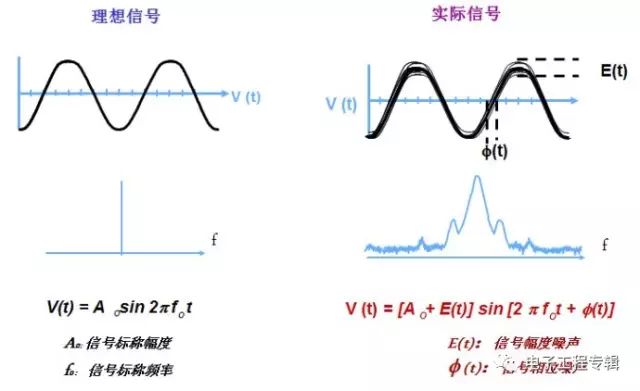
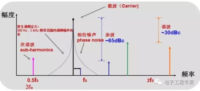
Figure 4 Signal characteristics of the actual sine wave
The evaluation of the quality of a sine wave or continuous wave signal is mainly performed in the frequency domain, and the spurs in the frequency domain contain continuous and discrete components, which all correspond to distortion in the time domain. The continuous noise sideband is called phase noise, and the discrete spurs are divided into harmonics and clutter according to their frequency relationship with the fundamental wave.
Phase noise is mainly caused by internal noise of the oscillator, and the formation of harmonic clutter is related to the nonlinearity of the device:
Vo(t)=a1vi(t)+ a2vi2(t)+ a3vi3(t)+ ...
If the input is an ideal sinusoidal signal, the output through nonlinear action is:
Vo(t)=a1sin(wt)+ a2sin2(wt)+ a3sin3(wt)+ ...
=a2/2+ a1sin(wt)+ 3a3/4sin(wt)+ a2/2sin(2wt) + a3/4sin(3wt) + ...
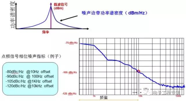
Figure 5 Phase noise definition of a sinusoidal signal
The phase noise indicator is mainly described in the frequency domain, and is represented by a single sideband (SSB) noise power spectral density and carrier power ratio under a certain offset. The frequency offset range of the project is: 10Hz~1MHz, and the frequency offset horizontal coordinate is expressed by logarithm.
Second, the point frequency signal sourceIn general, the point frequency signal source consists of three parts:
1. Reference source section: Determine the overall signal source frequency stability;
2. Frequency synthesis part: determine the output signal frequency parameter;
3. Output power control part: determine the output signal power parameter
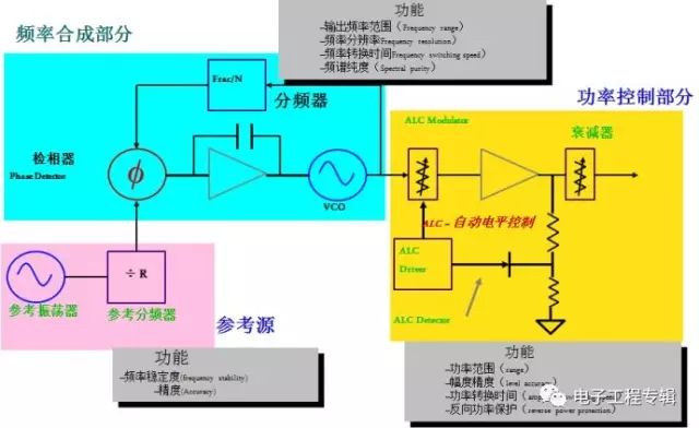
Figure 6 signal source composition block diagram
The technique of synthesizing signals that meet the requirements of various indicators is called frequency synthesis technology. There are three main ways to synthesize signal frequencies:
Direct frequency synthesis
The oscillator directly outputs the required frequency signal, and the crystal oscillator is widely used due to its high Q value. The constant temperature crystal oscillator and the steady crystal oscillator can further improve the frequency stability. Mainly used in single point frequency signal synthesis.
2. Indirect frequency synthesis
The frequency synthesis is performed by using a PLL phase-locked loop, which is characterized in that it can output a wide frequency range signal, the frequency change step is small, and the frequency jump speed is fast. However, there are disadvantages in that the frequency variation step and the phase noise index are contradictory. PLL indirect frequency synthesis is the main method of frequency synthesis.
3. Direct Digital Synthesis (DDS)
The use of digital technology for signal waveform synthesis is characterized by a high output frequency step index, a fast frequency jump, but a narrow output frequency range.
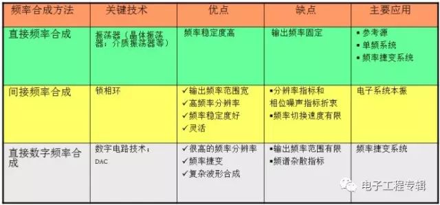
Figure 7 Signal source frequency synthesis technology and its advantages and disadvantages
The block diagram of the direct frequency synthesis technique is shown in the figure below. The temperature stability of the crystal oscillator can be improved by using a temperature-compensated crystal oscillator and a constant-temperature crystal oscillator.
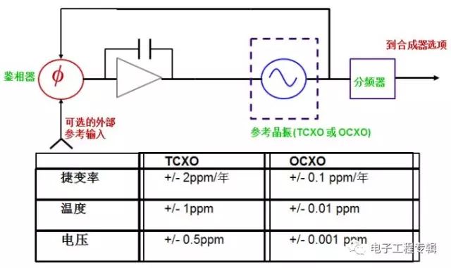
Figure 8 Block diagram of direct frequency synthesis
The block diagram of the indirect frequency synthesis technique is shown in the figure below. The phase-locked loop is composed of a phase detector, a loop filter, a voltage controlled oscillator (VCO), a frequency divider, and the like.
From the frequency relationship analysis, the PLL is equivalent to a frequency multiplier: the PLL output signal frequency change step is its phase detector operating frequency.
If the frequency change step is required to be smaller, the phase discrimination frequency is correspondingly smaller, and the output frequency value is required to be correspondingly larger. A smaller phase-detection frequency will result in a corresponding reduction in the PLL loop bandwidth, which will degrade the PLL dynamic performance (frequency hopping speed).
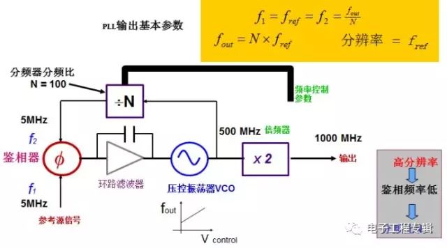
Figure 10 Block diagram of indirect frequency synthesis
The phase noise indicator of the PLL output signal is analyzed.
For the reference source, the PLL is low-pass and the bandwidth is loop bandwidth. The phase noise of the PLL output is that the phase noise of the reference signal is degraded by N times. The larger N is, the worse the PLL output phase noise index is. Outside the loop bandwidth, the PLL output phase noise is determined by the VCO.
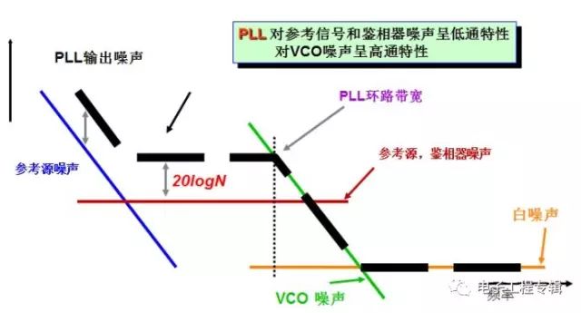
Figure 11 Phase-locked loop output phase noise indicator
The principle of improving the phase noise index of the PLL output signal is to reduce the frequency division ratio N, which can be achieved by using a multi-phase locked loop and a fractional frequency division technique.
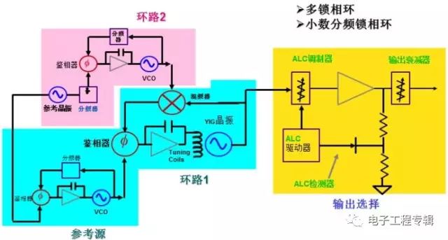
Figure 12 Method for improving phase noise of PLL output signal
Direct digital frequency synthesis DDS is a new technology that emerged with the development of digital technology. The principle block diagram is shown below. The DDS consists of a phase accumulator; a ROM table; a DAC; a low pass filter.
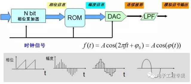
Figure 13 DDS direct digital synthesis technology block diagram
The signal source uses ALC (Automatic Level Control) technology to ensure the amplitude of the output signal. A wide range of amplitude adjustments is done by the attenuator.
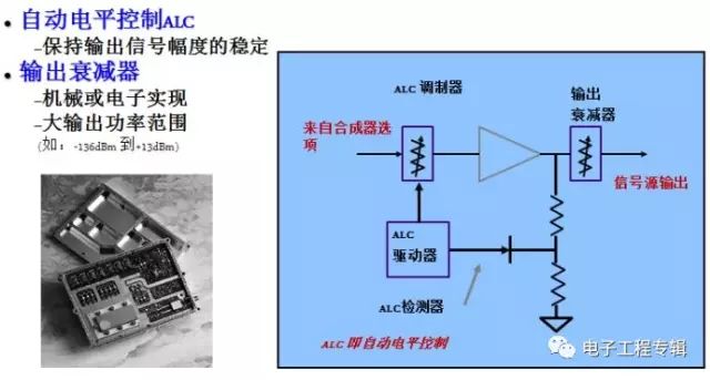
Figure 14 Control of signal source output signal power
Application of point frequency signal source:
1. System local oscillator: – phase noise – frequency accuracy 2. device distortion performance test – spur – third-order distortion TOI 3. receiver test: – modulation mode – amplitude accuracy – spurious performance
The general point frequency signal source has scanning functions, including: frequency scanning function and power scanning function.
There are two ways to scan for frequency: step scan and list scan. Frequency scanning requires attention: level accuracy, flatness, source matching.
Step scan needs attention: accuracy, number of scan points, switching time. List scanning needs attention: accuracy, switching time, dwell time.
Power scanning requires attention: power sweep range, power slope range, source match. Power sweep is accomplished by: automatic level control ALC, ALC detector, ALC driver and ALC modulator.
Third, the analog signal generator is the analog modulation signal sourceThe modulated signal can be classified into analog modulation and digital modulation according to the difference of its modulation signal.
The sine wave signal contains three independent parameters, amplitude, frequency and phase. If a continuous sine wave is unmodulated, then its envelope amplitude, vibration frequency, and initial phase will always be a constant (regardless of noise factor), and such sinusoidal information is zero. Our traditional analog modulation is to use the modulation signal to change these three parameters of the carrier, so that the carrier carries the modulated information from one end to the other.
Why is the modulated signal modulated onto the carrier? The function of the carrier is to use a higher RF or MW frequency as the carrier, so that the information will spread farther. For example, using baseband propagation, the distance will generally be as close as possible. For example, you use the telephone and the building. Other colleagues are more convenient and labor-saving than yelling at you in the hallway. Many people imagine digital modulation is a new technology, but in fact all modulation methods can be summarized as basic AM, FM and PM.
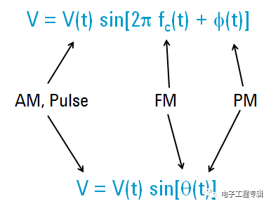
Figure 15 Position of the modulation information AM signal requires the following parameters: 1. Carrier frequency 2. Modulation signal frequency 3. Modulation index
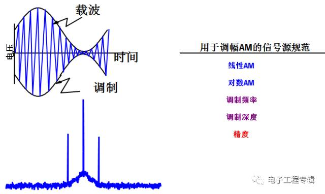
Figure 16 amplitude modulation AM
The FM FM signal requires the following parameters:
Carrier frequency
2. Modulation signal frequency 3. Modulation frequency offset 4. Modulation index
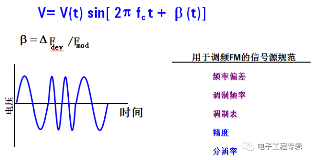
Figure 17 Frequency Modulation FM
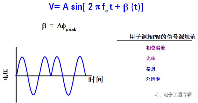
Figure 18 Phase Modulation PM
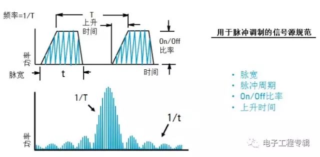
Figure 19 Pulse Modulation
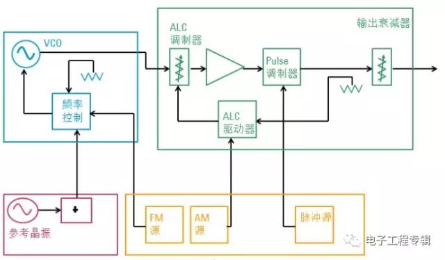
Figure 20 Analog modulation signal source block diagram 3, vector signal generator is the digital modulation signal source
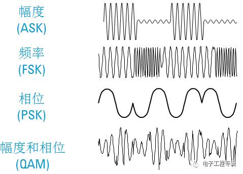
Figure 21 Waveform comparison of various modulation methods It is very convenient to describe a sine wave with a vector. In polar coordinates, the vector represents the relationship of the peak voltage amplitude of the sine wave to the amount of phase change. A phase rotation of 360 degrees represents a complete frequency cycle. Note that the opposite sign provides a convenient way to indicate that the sine wave phase changes over time. The oscilloscope in the figure shows the process of a signal amplitude as a function of time. Vectors cannot provide any frequency information directly. In fact, we measure the reference phase of the vector relative to the carrier signal. This means that the vector will only rotate when the frequency is different.
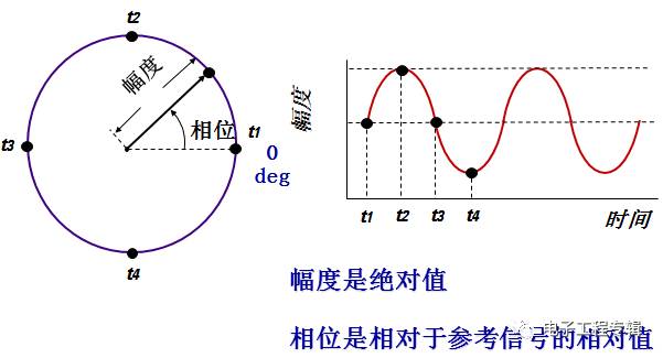
Figure 22 In the polar coordinates, a vector is used to describe a sine wave. The following examples of various modulation signals are shown in the I/Q plane. Understand them, you understand all the I/Q modulation principles. In any I/Q diagram, the amplitude of the signal as it is changed in the radial direction means that the phase of the signal is changing (and only the phase changes). So AM modulation, only the vector radial variation in the I / Q diagram. PM modulation is a vector rotation. FM looks like PM because the deviation from the carrier frequency is the change in phase per unit time. Remember that both amplitude and phase variations are relative to the unmodulated carrier. The Vectordiagram is an intuitive way to describe the trajectory of a vector signal.
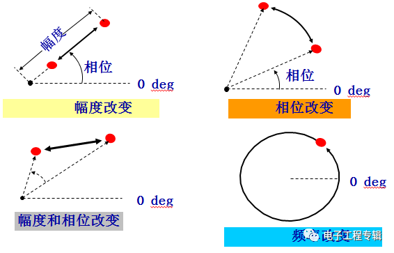
Figure 23 Signal changes in polar coordinates
Direct measurement of the phase of the vector is more difficult. The actual receiver and measurement system uses I/Q demodulation. It converts the control problem of the signal phase into a control problem of two orthogonal component voltages.
First, because it is simple, the interface is simple, the circuit is simple, and the baseband is simple to implement. Second, I/Q represents the orthogonal variable to the modulated signal, and the phase shift of one signal relative to the carrier by 90 degrees. If only the I channel is detected, due to COS ( 90°)=0, although the input signal exists, but the I channel output is 0V, then the I channel has no output signal. Therefore, by measuring the in-phase and quadrature components of the signal separately, we do not need to directly measure the relative phase of the signal.
The I/Q demodulator can measure amplitude and phase. What about the frequency parameter? The frequency is the phase versus time change, and the I/Q demodulator actually measures all types of modulation directly rather than just the AM, PM, FM modulated signals.
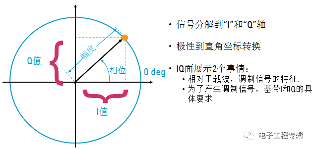
Figure 24 IQ format coordinates
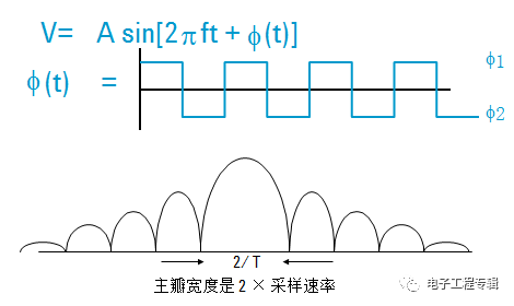
Figure 25 BPSK time domain frequency domain characteristics
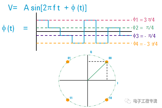
Figure 26 QPSK Time Domain and Constellation Mapping One way to observe digitally modulated signals is to use an eye diagram. Two different eye diagrams can be generated, one for I channel data and the other for Q channel data.
The eye diagram repeatedly displays the I and Q amplitude versus time in an infinitely continuous manner. The I and Q transitions can be displayed separately, forming an "eye" at the moment the symbol is determined. QPSK has 4 different I/Q states, each in one quadrant. I/Q each have two levels, forming one eye for each I and Q. The next picture is an example of 16QAM, with 4 levels enclosing 3 eyes. It is important to understand the concept of eye diagrams. A good signal has a "large" eye, and the intersection corresponds to the position of the symbol point on the constellation. The higher the modulation quality, the more concentrated the intersection.
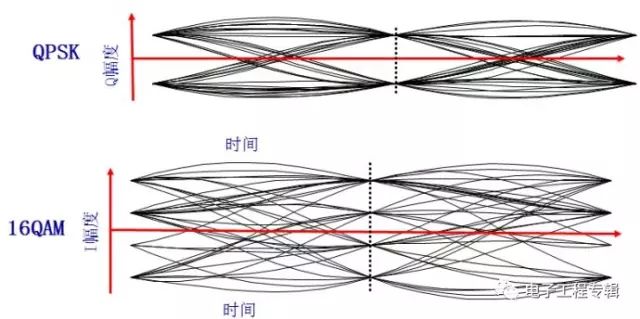
Figure 27 I and Q eye diagram
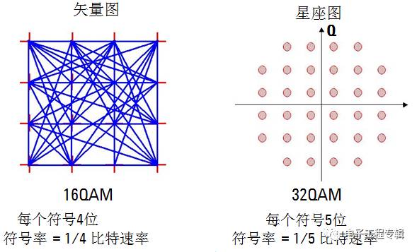
Figure 28 QAM vector and constellation
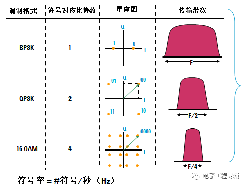
Figure 29 Comparison of vector modulation features
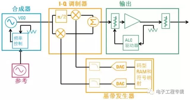
Figure 30 Block diagram of the vector signal generator
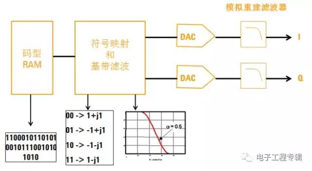

Figure 31 Baseband Signal Generator in Vector Signal Generator
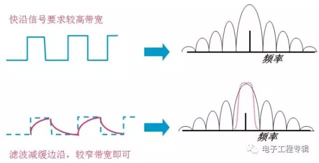
Figure 32: Filter in the baseband signal generator. IQ modulator: I and Q signals are synthesized by the same local oscillator signal, but the local oscillator has a 90-degree phase shift, and the I/Q paths do not interfere with each other. Finally, a sum signal is obtained. .
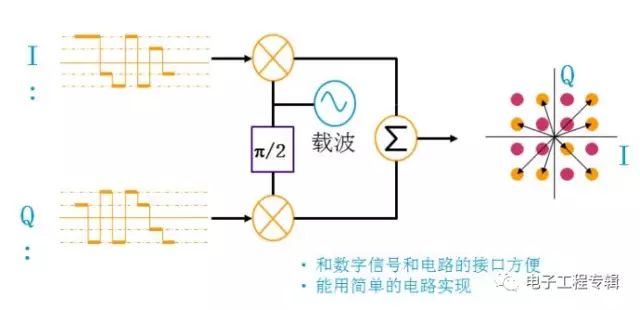
Figure 33 The main application of the IQ modulator vector signal generator in the vector signal generator:
Generate vector signals in a specific format
Receive sensitivity measurement
Receiver gating measurement
Device distortion measurement
Office Lighting Led Driver
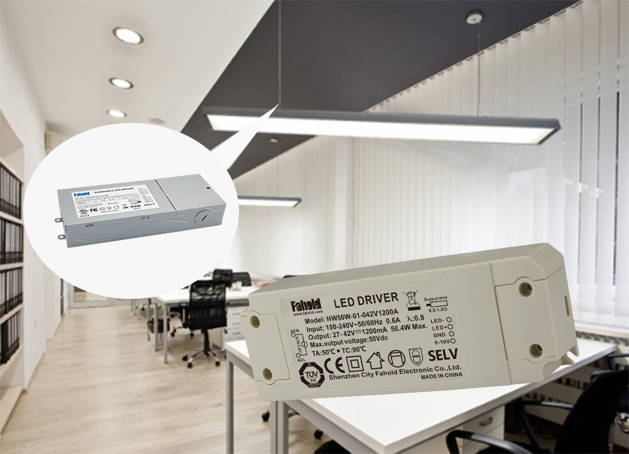
A comprehensive series of Office lightings drivers, suitable for use in a range of Office Lighting applications, including meeting room Lighting, Production line Lighting, Medical Lighting, Transportation Lighting, Entertainment Lighting, etc. We have skilled engineers to answer all your questions and enquiries and provide all-round solutions basis on your project(s) and provide technical supporting.
Specifically for office lighting, Generally used in the panel more, instead of the traditional lamp, but no flicker power, long hours of office work on the great damage to the glasses. Power requirements are not waterproof, high PF value, long life.
Input voltage: 100-277vac / 100-240vac / 100-130vac / 180-240vac / 100-347V
output voltage: 25-40vdc / 27-42vdc / 35-45vdc / 50-70vdc / 12Vdc / 24vdc
current: 100mA-8000mA.
Power factor: >0.9
Dimming:0-10V / PWM / RX / DALI.
>=50000hours, 3-5 years warranty.
certificate: UL CE FCC TUV SAA ect.
What's the benefits of Fahold Driver?
- Standard Linear Lighting
- Cost-effective led driver solution for industry,commercial and other applications
- Good quality of led driver with high efficiency output to meet different requirements
- Easy to order and install,requiring less time,reducing packaging waste and complexity
- Flexible solution
FAQ:
Question 1:Are you a factory or a trading company?
Answer: We are a factory.
Question 2: Payment term?
Answer: 30% TT deposit + 70% TT before shipment,50% TT deposit + 50% LC balance, Flexible payment
can be negotiated.
Question 3: What's the main business of Fahold?
Answer: Fahold focused on LED controllers and dimmers from 2010. We have 28 engineers who dedicated themselves to researching and developing LED controlling and dimming system.
Question 4: What Fahold will do if we have problems after receiving your products?
Answer: Our products have been strictly inspected before shipping. Once you receive the products you are not satisfied, please feel free to contact us in time, we will do our best to solve any of your problems with our good after-sale service.
48W Led Driver,Led Driver 700Ma,Led Dimming Driver
ShenZhen Fahold Electronic Limited , https://www.fahold.net