The ADS1256 is a micropower, high precision, 8-channel, 24-bit delta-sigma high performance analog-to-digital converter (ADC) from TI's Burr-Brown product line. The device offers up to 23 bits of noise-free accuracy, data rates up to 30kSPS (sub-samples per second), 0.0010% nonlinearity (maximum) and numerous on-board peripherals (input analog multiplexers, input buffers, Programmable gain amplifiers, programmable digital filters, etc.) provide designers with a complete, high-resolution measurement solution. The ADS1256 is available in a SSOP-2 package and is priced at $8.95 in 1,000-unit quantities.
Main features of ADS12561, 8 channel input: 8 channels of signal input can be collected at the same time.
2, wide measurement range: the basic range is 0-5V input voltage, can be welded at the input end of the voltage divider resistor, the voltage is adjusted to 0-5V, so the acquisition card can capture most of the standard voltage on the market,
3. The acquisition frequency is high and the precision is high: the acquisition rate of the acquisition card is 30K/s, and the precision can reach 0.00001.
4, industrial application level wiring, mold ground, digital ground completely isolated, strong anti-interference ability.
5, small size, easy to install applications
6, jump cap design, convenient multi-state combination
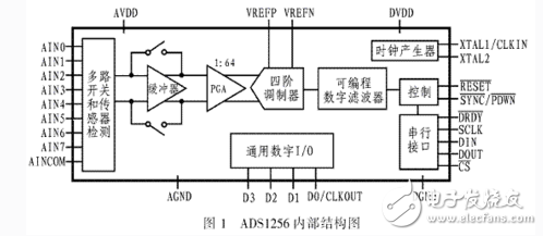
ADS1256 internal structureThe internal structure of the ADS1256 is shown in Figure 1. The device is mainly composed of analog multiplexer (MUX), input buffer (BUF), programmable gain amplifier (PGA), fourth-order delta-sigma modulator, programmable digital filter, clock generator, controller and serial SPI interface and other components. Since the ADS1256 provides nine analog inputs, it can be configured as a 4-way differential input, an 8-way unipolar input, or a combination of differential input and unipolar input using an analog multiplexer register. When analog input channel 0 is selected as the positive differential input (AINP), the remaining channels can be selected as the negative differential input (AINN). Generally, there is no limit to the choice of input pins, but for best analog performance, the following pin connections are recommended:

1. For differential measurement, AIN0~AIN7 are generally used as input terminals, and AINCOM is not used;
2. For unipolar measurement, AIN0~AIN7 are generally used as unipolar input terminals; AINCOM is used as a common input terminal, but AINCOM is not grounded;
3. Leave the unused analog input pins floating, which will help reduce the input leakage current.
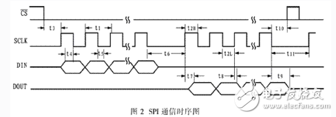
How ADS1256 worksThe ADS1256 uses a four-wire system (clock signal line SCLK, data input line DIN, data output line DOUT, and chip select line CS) SPI communication mode, which can only work in the slave mode of SPI communication. The design can control the ADS1256 on-chip registers through various host controllers (such as microcontrollers) and read and write these registers through the serial port. When serial communication is performed, CS must be kept low. The DRDY pin is used to indicate that the conversion has been completed. The latest conversion data can be read from the DOUT pin by the RDADA or RDATAC command. In the SPI communication process, data can be sent and received synchronously, and the data can also be moved synchronously using SCLK and DIN and DOUT signals. The SCLK signal should be kept as clean as possible to avoid data errors. On the rising edge of SCLK, data can be sent to the ADS1256 via DIN, while on the rising edge of SCLK, data can be read from the ADS1256 through DOUT. DIN and DOUT can also be connected to the main controller via a bidirectional signal line, but in this case, the RDATAC command must not be used to read the data. Figure 2 shows the timing relationship of the SPI communication.

The ADS1256 has four general-purpose digital I/O ports, all of which can be set to input or output through the IO registers. The input or output of each pin is set by the DIR bit of the IO register; the DIO bit is used to control the state of each pin. A clock generator can be set through the D0 pin for use by other devices (such as a microcontroller). This clock can be set to fCLKIN, fCLKIN/2, fCLKIN/4 by the CLK0 and CLK1 bits in the ADCON register. Using D0 as a clock increases the voltage consumption. Therefore, if the clock output function is not required, it is best to disable it by writing to the ADCON register after power-up or reset. The unused IO pins can be used as input ground or as outputs, which helps to reduce power consumption.
The main clock of the ADS1256 can be provided by an external crystal or clock generator. When generated by an external crystal, the crystal on the PCB board should be as close as possible to the ADS1256. To ensure that it can oscillate and get a stable frequency, an external capacitor (usually a ceramic capacitor) can be used. The crystal frequency is generally chosen to be 7.68MHz (ie fCLKIN = 7.68 MHz).
The ADS1256 can be reset by reset pin RESET, RESET command and special serial communication clock SCLK. The ADS1256's synchronous operation is available in both the SYNC/PDWN pin and the SYNC command.
The ADS1256 working process is mainly established by setting 11 independent registers, including all the information that needs to be set, such as sampling speed, analog multiplexer, PGA setting, I/O selection, self-calibration, etc. Table 1 shows the main register states of the ADS1256, including: Status Register STATUS, Analog Multiplexer Register MUX, AD Control Register ADCON, and Data Speed ​​Register DRATE.

Among them, the status register STATUS (address 00h, reset value X1H) of the upper four bits (ID bit) is set by the factory, ORDER bit is the data output order selection bit, when 0, the data output high bit first (default); At 1 o'clock, the data output is low first. The ACAL bit is the auto-calibration selection bit. When 0, the auto-calibration is off (default); when 1, the auto-calibration is on. The BUFFER bit is the input buffer selection bit. When 0, the input buffer is off (default); when 1, the input buffer is on. The DRDY bit is the conversion data status bit. This bit completely copies the state of the DRDY pin. When DRDY is low, it indicates that the data conversion is over, and the result can be read. When the high level indicates that there is no data conversion or data is being converted, it cannot be read at this time. data.
Pcb Terminal Block,Pcb Barrier Terminal Blocks,Pcb Terminal Block Connector,Barrier Terminal Blocks And Connectors
Sichuan Xinlian electronic science and technology Company , https://www.sztmlchs.com