The following is a simple example of the application of SERDES FPGAs in high-speed systems for communications and consumer applications, thereby expanding our horizons. Limited to the subject and length, the content can not be deep, I hope that interested readers refer to the relevant articles on the website. The high-speed standards and parametric features supported by Altera's Stratix GX are shown in the figure.
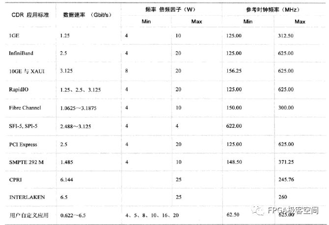
High-speed standards and parametric features supported by Altera's Stratix GX
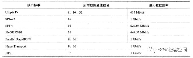
The Stratix IV high speed LVDS port features are shown in the figure.
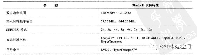
StratixIV supports high speed standards as shown.
Stratix IV GX supports such a wide range of high-speed standards, making Altera FPGAs widely used in high-speed systems. Traditional SERDES applications are mainly concentrated in the communication network as shown in the figure, especially in the fields of transmission, switching, access, etc., such as SONET/SDH, DWDM, Optical Switching, Router, CMTS, DSLAM, ATCA, SAN, 3G Mobile, etc. Backplane or line card. With the development of multimedia services and consumer electronics, SERDES is gradually being applied to digital TV broadcasting, video on demand and other fields. The following is an example of some high speed systems that use SERDES.
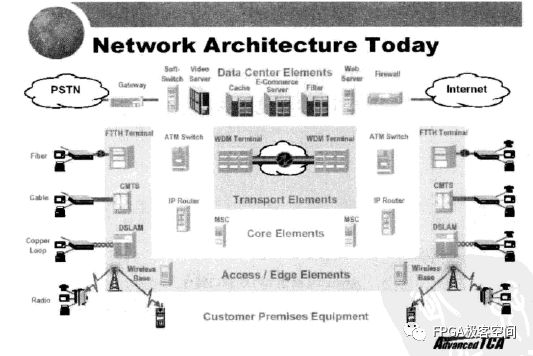
Schematic diagram of contemporary communication and data network structure
(1) The application of embedded SERDES FPGA in backplane or chip interconnect interface conversion.
The most common application for FPGAs with embedded SERDES is the conversion of the backplane or chip interconnect interface. In this example, the conversion of two 10G interfaces on the backplane enables XAUI to SP14.2 interface conversion through an embedded high-speed SERDES FPGA, as shown in the figure. In particular, Altera's Stratix IV embedded DPA functionality is very useful for implementing the complex interface SP14.2.
Converting XAUI to SPI4.2 interface on the backplane using SERDES
(2) The application of embedded SERDES FPGA in ATCA.
It can be seen from the structure of the contemporary communication network shown in the figure that the communication interfaces of different levels and different application fields in the communication network are complicated, and the solutions provided by different chip and device manufacturers are various, so in the communication room, different The interconnectivity of the manufacturer's boards and systems is poor, which is not conducive to development and maintenance. In order to make the communication interface efficient and uniform, PICMG (Global Industrial Computer Manufacturing Organization) provides ATCA. ATCA (Advanced Telecom Computing Architecture), the PICMG3 standard, provides a cost-effective, modular architecture, compatibility, and scalable hardware architecture for next-generation converged communications and data networking applications, while ATCA The development of modern transmission requirements and applications is also well supported in a modular structure. After adopting the ATCA architecture, the future communication network and data network will evolve into the structure shown in the figure, and further evolve into the idealized structure shown in the figure.
Schematic diagram of future communication and data network structure
The following sub-protocols are specified in the ATCA system.
PICMG3.1: Ethernet and Optical Switch Fabric.
PICMG3.2: Infiniband Switch Fabric.
PICMG3.3: StarFabric switch Fabric.
PICMG 3.4: PCI Express.
PICMG3.5: Rapid IO.
Each sub-criteria can be said to be a typical application based on high-speed SERDES.
High-end FPGAs embed the development trend of hard cores such as SERDES. High-speed SERDES broadens the data transmission bandwidth of FPGAs. Large-scale FPGAs provide flexible and fast choices for system-level solutions. In the high-speed ATCA field, embedded SERDES FPGAs will play an unprecedented role.
(3) The application of embedded SERDES FPGA is mainly limited to the field of communication, especially in the fields of transmission, switching, access, mobile, etc. With the continuous development of consumer demand, SERDES high-speed system has been widely used in traditional consumption. . As shown in the figure, a schematic block diagram of a digital television (DTV, Digital TV) data broadcasting system, the system solution using the embedded FPGA to participate in the DTV has the following advantages.
The flexibility of the FPGA and fast market response make it suitable for evolving standards and the need for continuous market innovation.
The FPGA's embedded high-speed SERDES or high-speed I/O ports enable implementations such as SMPTE-259M (360 Mbit/s) and SMPTE-292M (1.485 Gbit/s and 1.843 Gbit/s) and DTV data interface standards.
The development trend of embedded DSP or CPU processor in FPGA better supports video and voice processing, and provides better cost performance for FPGA to solve DTV system.
Schematic diagram of digital TV data broadcasting system
Round Male Pin Header Connectors
Round Male Pin Header Connectors,Straight Pin Male Pin Header Connectors,Straight Male Pin Header Connectors,Pitch Pin Connector
Dongguan ZhiChuangXing Electronics Co., LTD , https://www.zcxelectronics.com